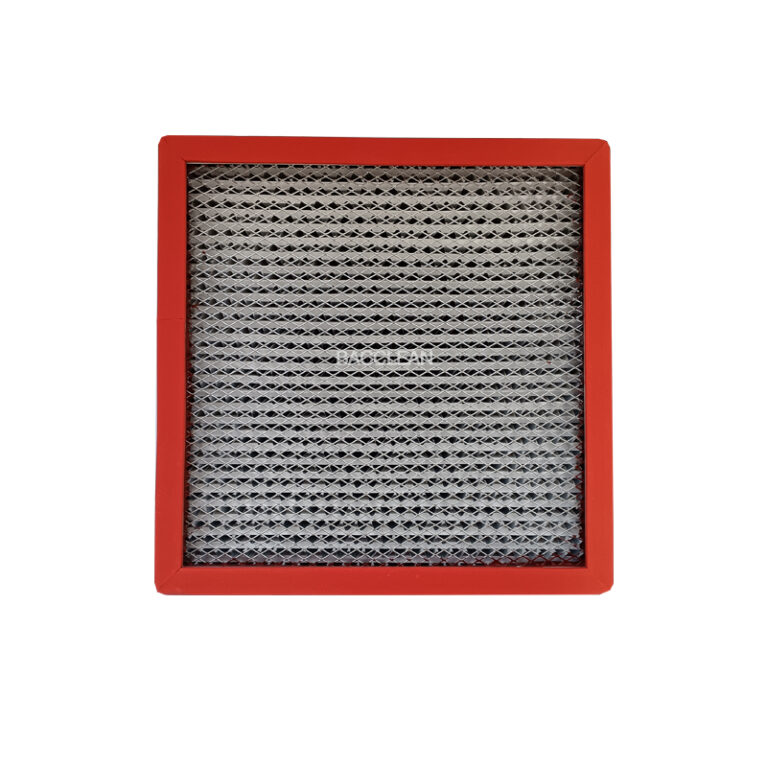
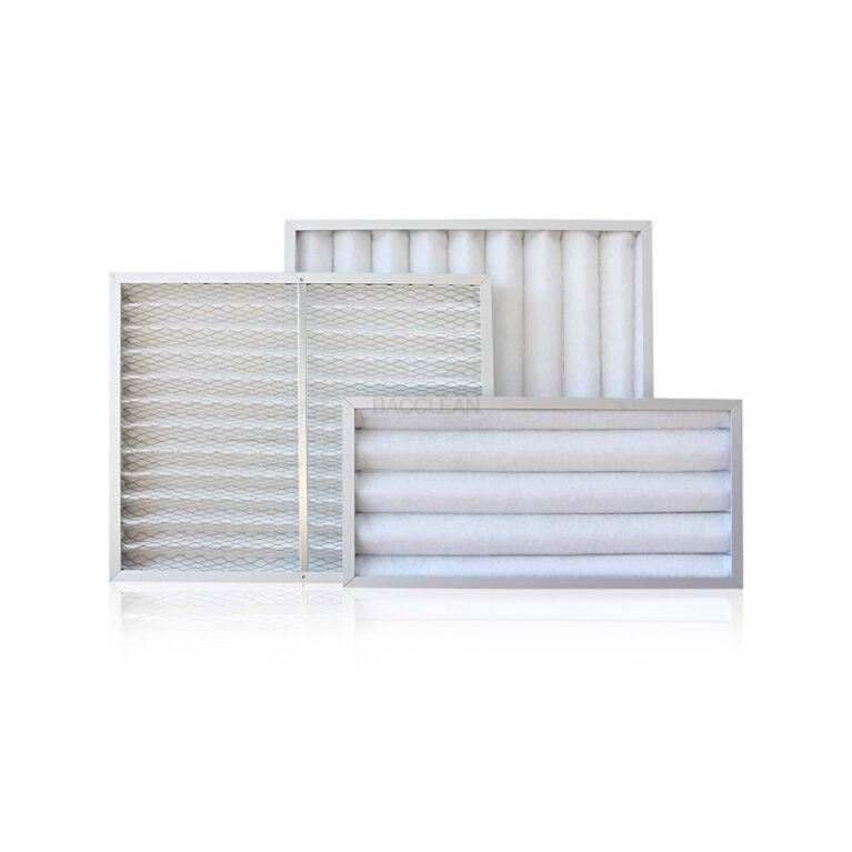
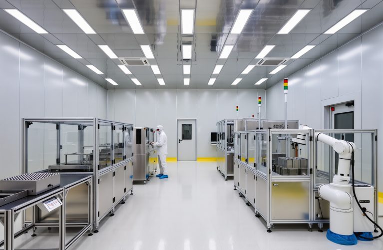
In the semiconductor field, FFU (Fan Filter Unit) is essential for maintaining the cleanliness of the core production environment. By driving airflow with a built-in fan through HEPA or ULPA filters, FFUs remove particles, dust, and microorganisms, creating a stable “local clean space” for manufacturing. Due to stringent cleanliness requirements (e.g., 12-inch wafer lines often require Class 1–10 cleanrooms), FFUs are used throughout chip production from front-end wafer manufacturing to back-end packaging and testing. The specific scenarios and values are as follows:
To understand the application value of FFU, it is important to examine how it supports different stages across the entire semiconductor manufacturing process.
Different stages in semiconductor manufacturing have varying requirements for cleanliness, airflow stability, and temperature and humidity. FFU, through flexible deployment and parameter adaptation, meets the strict requirements of each stage. Its main application scenarios include:
1. Front-end Wafer Fabrication: Core contamination control area
Front-end manufacturing is the stage with the highest cleanliness requirements in the semiconductor process (requiring Class 1 to Class 10). During the processes of photolithography, etching, thin film deposition (PVD/CVD), ion implantation, and cleaning of wafers, Even extremely small particles (such as those below 0.1μm) or metal impurities can cause chip defects (such as lithography pattern offset and thin film layer contamination). The application of FFU focuses on “local cleanliness enhancement around the equipment” :
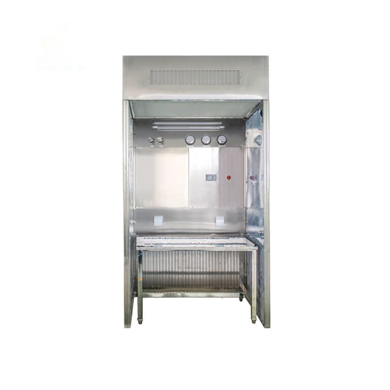
Lithography area: Lithography equipment (such as ASML lithography machines) is the core of wafer manufacturing, and its optical system and wafer stage are extremely sensitive to particles. FFU is usually directly deployed above the photolithography machine in the form of a “laminar flow hood”, forming a vertical downward “unidirectional clean airflow”, which forcibly carries away the particles around the equipment, preventing them from adhering to the wafer surface or optical lenses, and ensuring the photolithography accuracy (for example, the line width error of 7nm/5nm processes needs to be controlled at the nanometer level).
Etching/thin film deposition zone: During the operation of etching machines and PVD/CVD equipment, process dust (such as etching residues) may be generated. The FFU needs to be linked with the exhaust system of the equipment to balance the local pressure through a stable clean air flow, prevent process dust from spreading to the wafer surface, and at the same time avoid external contaminants from entering the equipment cavity.
Cleaning area: After the wafer is cleaned, its surface is in an “unprotected state” and is prone to secondary contamination by particles or organic pollutants in the air. The FFU is deployed above the transfer track at the outlet of the cleaning machine, forming a “clean air flow barrier” to ensure that the wafers remain clean during the transfer from cleaning to the next process.
2. Back-end Packaging & Testing: Balancing cleanliness and efficiency
The back-end processes (such as wafer thinning, dicing, bonding, packaging, and final testing) have slightly lower cleanliness requirements than the front-end (typically Class 100 to Class 1000), but they need to balance cleanliness and production efficiency. The application of FFUs mainly focuses on “area cleanliness division” :
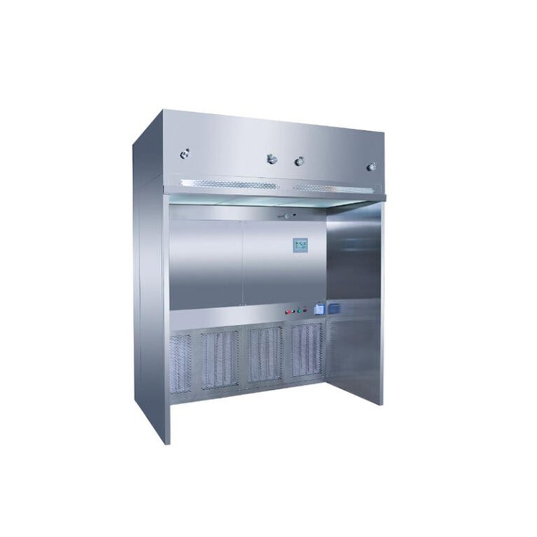
Scribing/bonding zone: Silicon dust is generated when the wafer is scribing (cut into bare chips), and it is necessary to avoid particles affecting the bonding accuracy during bonding (such as gold wire bonding, copper pin bonding). The FFU is deployed on the workbenches of the dicing machine and the bonding machine in the form of a “local clean unit” to filter dust and contaminants in a directional manner, while not affecting the automated operation of the equipment (such as the mechanical arm picking up and placing chips).
Packaging/final test area: During the packaging process (such as plastic packaging, pin forming), it is necessary to prevent resin impurities or environmental particles from entering the package body, which may cause short circuits or performance failures of the chip. In the final testing stage (such as electrical performance testing), it is necessary to avoid particles affecting the contact between the test probe and the chip pins. FFU is usually combined with a Clean Booth in this area to form a “modular clean space” that can be quickly set up, reducing the overall construction cost of the clean room.
In addition to core production areas, FFUs are deployed in various auxiliary spaces, further expanding their utility within semiconductor factories.
Wafer/mask storage area: Wafers (especially unprocessed bare wafers) and masks (the “pattern templates” used in photolithography) should be kept away from long-term exposure to contaminated environments during storage. Ffus are deployed in storage cabinets or storage rooms to maintain a Class 10 cleanliness level to prevent particle adhesion and subsequent process defects.
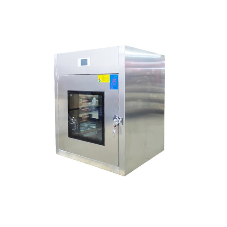
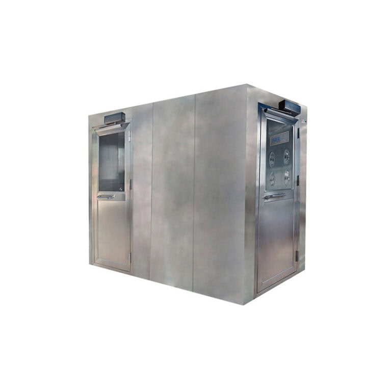
Equipment maintenance area: The maintenance of semiconductor equipment (such as photolithography machines and etching machines) must be carried out in a clean environment (to avoid the introduction of contaminants during maintenance). The “temporary clean maintenance space” set up by FFU can meet this requirement, eliminating the need to move the equipment to the core clean area and improving maintenance efficiency.
Ii. Core Technical Requirements of FFU in the Semiconductor Field
The particularity of semiconductor manufacturing places performance requirements on FFUs that far exceed those of ordinary industrial scenarios. The core technical indicators include
| Technical indicators | Requirement standards (Semiconductor scenarios) | Core meaning |
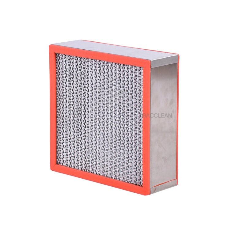
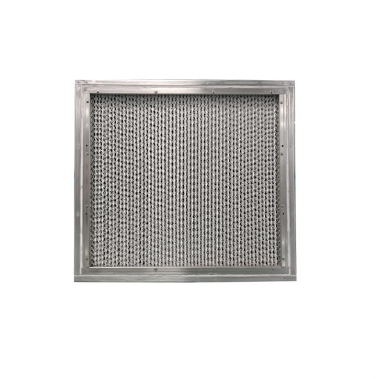
| Efficacité de la filtration | ULPA filters (with a filtration efficiency of ≥99.999% for 0.1μm particles) are required, and in some high-end scenarios, ULPA Class 150 (≥99.9995%) is needed. | Make sure to remove the most critical “sub-micron particles” in the semiconductor manufacturing process to avoid chip defects. |
| Airflow stability | The outlet air velocity fluctuation is ≤±0.1m/s, and the air flow uniformity is ≥90% (vertical laminar flow). | A stable airflow can prevent particles from “backflow” or “vortices”, and prevent contaminants from depositing on the wafer surface. |
| Low vibration/low noise | Operating vibration ≤0.5μm (amplitude), noise ≤55dB (A-weighted) | Semiconductor equipment (such as photolithography machines) is extremely sensitive to vibration (vibration can cause the photolithography pattern to shift), and low noise can ensure the comfort of operators. |
| Chemical corrosion resistance | The casing and internal components must be resistant to chemical gases used in semiconductor processes, such as fluorine, chlorine, and ammonia. | To prevent FFU components from being corroded by chemical gases, which could lead to particle shedding or equipment failure and pollute the production environment. |
| Intelligent monitoring and linkage | It supports real-time monitoring of wind speed, filter life, temperature and humidity, and can be linked with the factory MES system to achieve fault early warning and automatic adjustment | Semiconductor production requires continuous operation for 24 hours. Intelligent linkage can reduce manual intervention and avoid production halts caused by FFU failures. |
Iii. The Relationship between FFU and Semiconductor Cleanrooms: Optimization from “Global” to “Local”
Traditional semiconductor cleanrooms rely on a “central supply air + return air” system to maintain overall cleanliness, but they have problems such as high construction costs and difficulty in precisely controlling local cleanliness. The application of FFU has achieved an optimization mode of “global cleanliness + local enhancement” :
Cost optimization: The core production area (such as the lithography area) achieves Class 1 cleanliness through FFU, while other areas maintain Class 100 cleanliness. There is no need to build a high-level clean room as a whole, reducing construction and operation energy consumption (the energy consumption of FFU is only 60% to 70% of that of the central system).
Flexibility enhancement: FFU can be modularly deployed, and in combination with clean booths, the clean area can be quickly adjusted (such as adding FFU units when the production line expands), adapting to the rapid iteration requirements of semiconductor processes.
Controllable risk: If a certain FFU malfunctions and only affects a local area, it can be quickly switched through redundant FFUs (standby units) to prevent global cleanroom failure and production halt, thereby enhancing production stability.
Iv. Summary
The core value of FFU in the semiconductor field lies in “ensuring the overall process yield through local clean control” – by precisely removing sub-micron particles and maintaining a stable clean airflow, it provides reliable environmental protection for the key links in chip manufacturing. As semiconductor manufacturing processes advance towards 3nm and below (with cleanliness requirements raised to Class 0.1, that is, ≤0.1 0.1μm particles per cubic foot), FFU technology will be further upgraded. Such as integrating “static elimination function” (preventing particles from adhering to the wafer surface due to static electricity) and “AI adaptive regulation” (adjusting wind speed based on real-time contamination concentration), it continuously meets more stringent manufacturing requirements.